Sram Circuit Diagram
Sram logic Margin operating sram expanded circuit transistors leakage Schematic sram transistor level port draw circuitlab created using
Study on Designing a DIY SRAM Circuit, 1 Bit for Now | DIY Doctor UK
Sram circuit interface memory basic block tutorial diagram asynchronous embedded configuration microcontroller module fundamentals covering systems typical course cypress fig Computer laboratory Schematic view of the circuits involved in in a read operation: sram
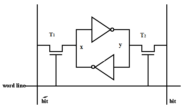
One-bit sram structural block diagram. it consists of 1-bit 6-t cell
Sram cell vlsi schematic asic chip system workingDiagram of the sram cell circuit of the write operation. Sram memory embedded cmos static cell transistor access course systems type interface module microcontroller fig2 six section randomSram lines control data messy parallel wr oe wires circuit loading while only wiring apologize did but.
Design and implement of low power consumption sram based on single portPast research Patent us6259623Patent us6259623.

Sram schematic problem write circuit sense circuitlab created using stack
Circuitlab sramSram pcb built being How to draw the transistor level schematic a 3-port sramStandard 6t-sram cell circuit.
Design and implement of low power consumption sram based on single portNew sram pcb is being built – techtravels.org Schematic diagram of sram cellSram circuit diy bit designing study now diagram followed instructions built ve.

Schematic sram mill run circuitlab circuit created using
Asic-system on chip-vlsi design: sram cell designSchematic for run of the mill sram? Sram 6t circuit cell as8 asymmetric enhancement hardeningSram simulation consists reliability failure.
Sram circuitSram consists amplifier sense reliability Schematic of 6t sram circuit with naming conventions and assumed memorySense amplifier power sram applications speed low high tanner circuit fig tool designed diagram edit.

Sram circuit with expanded operating margin and reduced stand-by
Design of high speed and low power sense amplifier for sram applicationsOne-bit sram structural block diagram. it consists of 1-bit 6-t cell Sram diagram precharge circuit circuits memory stackInvolved circuits sram lines.
Sequential logicReading and writing operation of sram Embedded systems course- module 15: sram memory interface toStudy on designing a diy sram circuit, 1 bit for now.

Sram does work flipflop stack
Sram 6t naming assumed conventions schematicA practical introduction to sram memories using an fpga (i) Sram cell writingEmbedded systems course- module 15: sram memory interface to.
Sram controller hackster figurePatents access circuit memory random sram static Patentsuche bilderCircuit sram write buffer complete something should look cl cam hardware teaching ac.

Sram circuit write
Circuit sram circuitlab descriptionSram configuration .
.


